LPDDR4X/LPDDR4 SDRAM
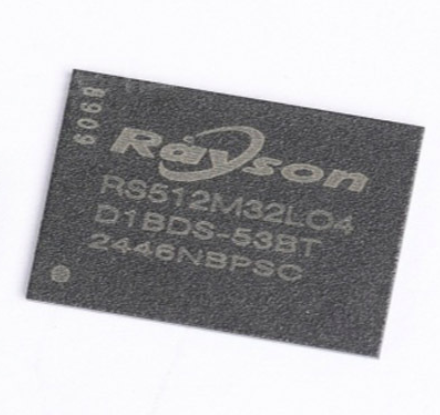
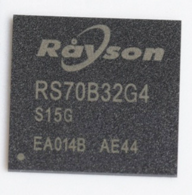
RS512M32LO4D1BDS-53BT、RS1G32LO4D2BDS-53BT
• Ultra-low-voltage core and I/O power supplies
– VDD1 = 1.70–1.95V; 1.80V nominal
– VDD2 = 1.06–1.17V; 1.10V nominal
– VDDQ = 0.57–0.65V; 0.60V nominal
or VDDQ = 1.06–1.17V; 1.10V nominal
• Frequency range
– 2133–10 MHz (data rate range per pin: 4266–20 Mb/s)
• 16n prefetch DDR architecture
• 8 internal banks per channel for concurrent operation
• Single-data-rate CMD/ADR entry
• Bidirectional/differential data strobe per byte lane
• Programmable READ and WRITE latencies (RL/WL)
• Programmable and on-the-fly burst lengths (BL = 16, 32)
• Directed per-bank refresh for concurrent bank operation and ease of command scheduling
• Up to 8.53 GB/s per die x16 channel
• On-chip temperature sensor to control self refresh rate
• Partial-array self refresh (PASR)
• Selectable output drive strength (DS)
• Clock-stop capability
• RoHS-compliant, “green” packaging
• Programmable VSS (ODT) termination
• Single-ended CK and DQS support
• VDD1/VDD2/VDDQ: 1.80V/1.10V/0.60V or 1.10V
• Array configuration
– 512 Meg x 32 (2 channels x 16 I/O)
– 1 Gig x 32 (2 channels x 16 I/O)
– 1536 Meg x 32 (2 channels x 16 I/O)
– 2 Gig x 32 (2 channels x 16 I/O)
• Device configuration
– 512M32 x 1 die in package
– 512M32 x 2 die in package
– 512M32 x 1 die and 1G16 x 2 die in package
– 1G16 x 4 die in package
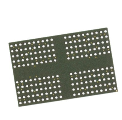
• FBGA “green” package
– 200-ball VFBGA (10mm × 14.5mm, seated height: 1.1mm MAX)
• Speed grade, cycle time
– 535ps @ RL = 32/36
– 468ps @ RL = 36/40
• Operating temperature range
– –25°C to +85°C